-

Dynabook Unveils Limited Edition 'Ghost in the Shell: Stand Alone Complex' Laptop
Dynabook announces a limited-edition 'Ghost in the Shell: Stand Alone Complex' laptop, blending iconic anime aesthetics with modern hardware and a full suite of custom accessories.
-

Samsung Reportedly Preps 1 Million Galaxy Wide Fold Units to Counter Apple's iPhone Fold
Samsung is reportedly preparing to launch its new Galaxy Wide Fold with an initial production run of one million units, setting the stage for a major foldable market showdown.
-

Vivo Unveils X200T: A Powerhouse with Dimensity 9400+, 6200mAh Battery, and Zeiss Triple Camera
Vivo has officially launched the X200T in India, a new mid-to-high-end smartphone powered by the MediaTek Dimensity 9400+ and featuring a versatile Zeiss-tuned triple camera.
-

Mouse Computer Unveils NEXTGEAR Case with Instantly Switchable Transparent-to-Frosted Glass
Japanese PC maker Mouse Computer has launched the innovative NEXTGEAR Clear Shift case, featuring a glass side panel that can instantly switch between transparent and frosted modes.
-

Samsung Unveils Special Edition Galaxy Z Flip7 for Milano Cortina 2026 Winter Olympics
Samsung has launched a special edition Galaxy Z Flip7 for the Milano Cortina 2026 Winter Olympics, featuring a unique gold and blue design for competing athletes.
-

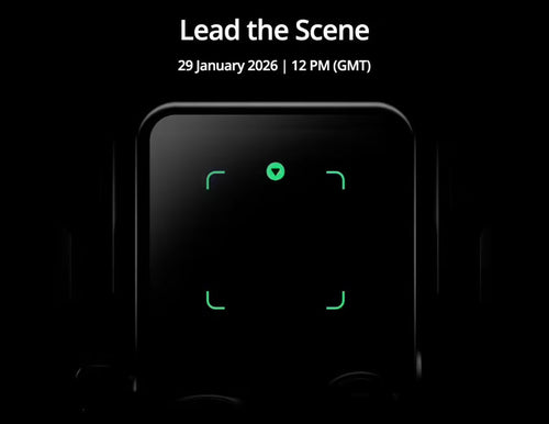
DJI Osmo Pocket 4 Leaks: 1-Inch Sensor, Dual-Camera Pro Model, and Jan 29 Release Date Revealed
Leaked posters reveal the DJI Osmo Pocket 4 series, featuring a Standard version with a 1-inch sensor and a powerful new dual-camera Pro model set for a later release.
-

Samsung's Next-Gen Galaxy Buds 4 Leaks, Revealing a Sleek New Design
Samsung's next-generation Galaxy Buds 4 series has been unofficially revealed through the company's own apps, showcasing a new, flatter stem design and hinting at numerous functional upgrades.
-

REDMI Turbo 5 Max Set to Dominate with a Mammoth 9000mAh Battery and Dimensity 9500s Chip
Leaked specs for the REDMI Turbo 5 Max reveal a massive 9000mAh battery, a powerful new chipset, and 100W fast charging ahead of its January 29th launch.
-

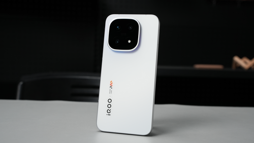
iQOO 15 Ultra Design and Specs Revealed: A Look at the 'Future Pod' and Snapdragon 8 Elite Gen5
First look at the iQOO 15 Ultra's official 'Future Pod' design and 'Energy Blade' lighting, plus a deep dive into its leaked powerhouse specifications.
-

Xiaomi Unveils Mijia Smart Head Massage Comb with Graphene Heating System
Xiaomi launches the Mijia Smart Head Massage Comb, a high-tech device for scalp care with graphene heating, app control, and a waterproof design for ultimate relaxation.
-

Keychron Unveils V Ultra 8K Series: 8000Hz Polling Rate and 660-Hour Battery Life
Keychron launches the V Ultra 8K series, offering tri-mode connectivity, an 8000Hz polling rate, ZMK firmware, and an incredible 660-hour wireless battery life for pro-level performance.
-

Priced at $400,000! Is the World's First Tri-Fold TV Hinting at the Next Battleground for High-End TVs?
Porsche Design and C SEED's $400,000 tri-fold TV is here, sparking a debate on whether innovative form factors will define the future of high-end television.
-

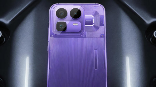
RedMagic 11 Air Hands-On: The Fan and Transparent Design Make a Triumphant Return
The RedMagic 11 Air marks the return of the iconic transparent back and built-in cooling fan to the brand's lightweight gaming phone series, packing flagship power and a massive battery.
-

Raspberry Pi Unveils Its First-Ever Official Flash Drive with a Focus on Performance and Reliability
Raspberry Pi introduces its official Flash Drive, a durable and high-performance USB-A storage solution available in 128GB and 256GB capacities, designed for reliability and speed.
-

Apple's New AI Hardware Leaked: A Successor to the iPhone or a Repeat of the Failed AI Pin?
Apple is secretly developing a wearable AI device reminiscent of the failed AI Pin, potentially bundled with iPhone 19. Is this a strategic hedge or the next big thing?
-

Redmi Buds 5 Pro Announced: Featuring a "Rare" Coaxial Triple-Driver System for Premium Sound
Redmi has officially unveiled the new Redmi Buds 5 Pro, featuring a groundbreaking coaxial triple-driver system, Spatial Audio, and Hi-Res wireless support for an unparalleled audio experience.
-

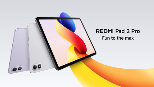
REDMI Pad 2 Pro Announced: A Powerhouse Tablet with a 12,000mAh Battery and 69-Day Standby
Xiaomi's new REDMI Pad 2 Pro is here, boasting an incredible 12,000mAh battery with 69-day standby, a large 2.5K display, and power bank capabilities.
-

Slimbook ONE Mini PC Gets a Major Upgrade with AMD Ryzen AI 9 HX 370 and OCuLink
Spanish PC maker Slimbook has refreshed its ONE mini PC, now offering powerful new AMD Ryzen CPU options, including the AI 9 HX 370, and versatile OCuLink connectivity.
-

The Off-Road Robot Vacuum: A Hands-On Look at the Roborock G30S Pro and its 8.8cm Obstacle-Climbing Power
Meet the Roborock G30S Pro. This 'off-road' robot vacuum features a revolutionary AI Wheel-Leg system, conquering obstacles up to 8.8cm while delivering a superior, automated cleaning experience.
-

Marshall Unveils Heddon Hub: Upgrade Your Bluetooth Speakers with Multi-Room Sync
Marshall introduces the Heddon streaming hub, a new device that adds multi-room synchronized playback capabilities to your existing Bluetooth speakers using innovative Auracast technology.
-

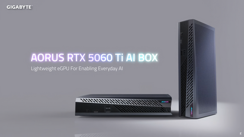
Gigabyte AORUS RTX 5060 Ti AI BOX Review: One Dock for Power, Transfer, and Performance
The Gigabyte AORUS RTX 5060 Ti AI BOX transforms thin laptops into performance powerhouses for gaming and AI, featuring Thunderbolt 5 and a desktop-class GPU.
-

Fujifilm's Instax mini Evo Cinema: The Most Fun Camera I Can't Recommend
A review of the Fujifilm Instax mini Evo Cinema. This camera is incredibly fun with a fantastic retro design, but its core technical flaws make it impossible to recommend.
-

Apple's First Wave of 2026 Products: Radical M5 MacBooks and a Game-Changing Budget Model
Apple's first 2026 wave includes new M5 Pro/Max MacBooks, a rumored budget model, and upgraded displays, set to shake up the PC market.
-

The Asian Robot Legion: Dominating Las Vegas at CES 2026
CES 2026 is dominated by a new wave of robots from Asia, spanning from humanoid workers and emotional companions to highly specialized cleaning bots conquering every corner.
-

Goodbye to the 'Brick' Phone! RedMagic 11 Air Hands-On: An Ultra-Slim Body with a Built-in Fan and an Incredible Feel
The RedMagic 11 Air challenges gaming phone stereotypes with its ultra-slim design, built-in fan, and incredible feel, offering top-tier performance without the bulk.
-

Insta360's Modular Pocket Gimbal Camera Prototype with Leica Lens Leaked
Leaked images reveal Insta360's groundbreaking modular pocket camera prototype. It features a detachable Leica lens module that can be attached to a gimbal for ultimate versatility.
-

Omdia Report: Vivo Dominates India's Smartphone Market in 2025 Amidst Overall Decline
Omdia's 2025 report highlights vivo's dominance in India's declining smartphone market, with a significant lead over Samsung and OPPO.
-

Pulsar Unveils 'Blue Archive' Themed X2 CrazyLight Mice Featuring Abydos Characters
Pulsar has announced a new collaboration with 'Blue Archive', releasing three special edition X2 CrazyLight mice themed after popular characters from Abydos High School.
-

DJI's Strategic Pivot: Is the Xtra ATTO a Rebranded Osmo Nano for North America?
DJI is rumored to be rebranding its popular Osmo Nano camera as the Xtra ATTO, a strategic move aimed at navigating potential US trade barriers.
-

Lenovo Idea Tab Pro Gen 2 Renders Leak, Revealing Sleek Redesign and Capsule Camera
Leaked renders reveal the Lenovo Idea Tab Pro Gen 2's new minimalist design, featuring a unique capsule camera, quad speakers, and a full suite of productivity accessories.
-

Realme Neo8 to Redefine Mid-Range Photography with 50MP Periscope Zoom
Realme is set to redefine mid-range photography, announcing the Realme Neo8 will feature a powerful 50MP periscope telephoto lens with an incredible 120x super zoom capability.
-

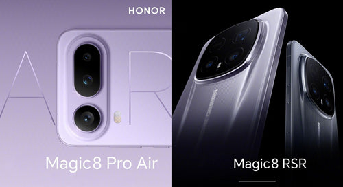
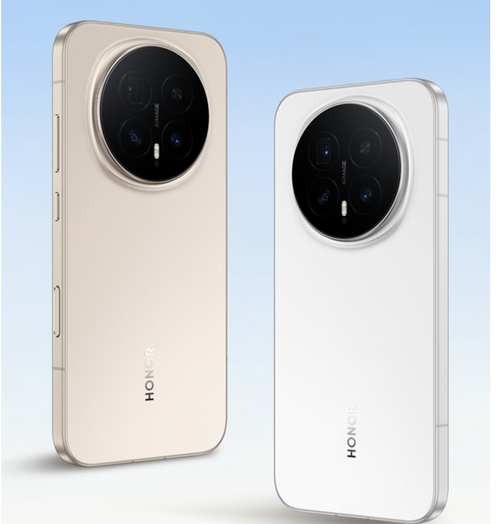
Honor's Dual Flagship Launch: The 'Pro First' Magic8 Pro Air and a New Porsche Design
Honor's latest launch introduces the Magic8 Pro Air, a 'Pro' level ultra-thin phone, and the Magic8 RSR Porsche Design, challenging market conventions with uncompromised specs.
-

Realme Buds Air6 Pro Unveiled: Pre-Orders Open for Earbuds with 55dB Deep Sea Noise Cancellation
Realme has announced its new Buds Air6 Pro, now available for pre-order. The earbuds boast powerful 55dB noise cancellation and are set to launch on January 22.
-

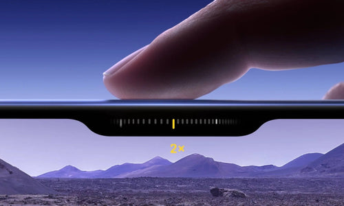
The Smartphone Telephoto War: Continuous Zoom vs. Dual-View vs. Dual 200MP
A battle for telephoto supremacy: continuous optical zoom, dual-view periscopes, and dual 200MP sensors. Discover which technology will define the future of smartphone photography.
-

Apple's Big Gambit: Partnering with Google Gemini to Reinvent Siri—A Challenge to Chinese Phones' AI Edge?
Apple's shocking alliance with Google to power Siri with Gemini AI threatens the long-held advantage of Chinese phone brands, potentially reshaping the entire mobile AI landscape.
-

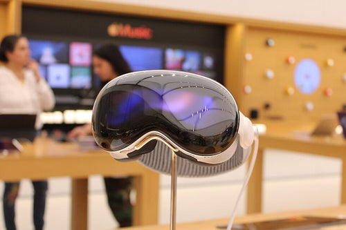
The End of an Era? Vision Pro Reportedly Halted as Apple's Spatial Computing Story Falters
With Apple's Vision Pro reportedly facing a production halt, we analyze the missteps that doomed the ambitious spatial computing device, from its staggering price to its closed ecosystem.
-

Realme Neo 8 to Make Global Debut with World-First 165Hz Samsung Display
The upcoming Realme Neo 8 is poised for a global debut, featuring a groundbreaking 165Hz Samsung display that promises an unparalleled visual experience for users.
-

RedMagic 11 Air Launch Set for January 20, Teasing Return of Cooling Fan and a 'True Full-Screen' Future
RedMagic will unveil the new RedMagic 11 Air on January 20, with rumors suggesting the return of its iconic cooling fan and a future full-screen display.
-

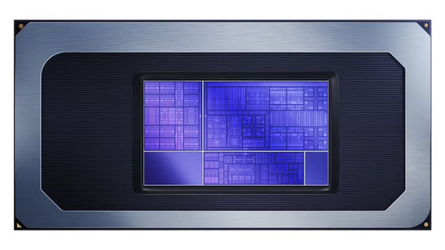
Leaked: Intel's New Core G3 Processor Aims to Power Next-Gen Gaming Handhelds
Intel is entering the handheld gaming scene with its newly leaked Core G3 processor, featuring a hybrid Panther Lake architecture and Arc B380 graphics for mid-range performance.
-

Redmi's Next Flagship Killer? Rumors Hint at a Dimensity 9500 Phone with Active Cooling and IP68
A new Xiaomi Redmi phone is reportedly in testing, rumored to feature the powerful Dimensity 9500 chip, a built-in cooling fan, and a surprising theoretical IP68 water resistance rating.
-

MSI Unveils Ultra-Slim Modern 14S and 16S Laptops at CES 2026
MSI launches its new Modern 14S and 16S mainstream laptops at CES 2026, boasting an incredibly thin and light design powered by next-generation Intel Core Ultra processors.
-

No More 'Small and Beautiful' Phones? ASUS Halts Mobile Business as Niche Brands Near the Edge
ASUS is halting its Zenfone and ROG phone lines, signaling a tough reality for niche smartphone brands in a market that prioritizes scale over unique design.
-

CES 2026: Samsung's Family Hub Refrigerators Get a Hands-Free Upgrade with Voice-Controlled Doors
Samsung's 2026 Family Hub refrigerators, unveiled at CES, feature voice-controlled doors and Gemini AI for a smarter, hands-free kitchen experience.
-

"AI in Every Product": Samsung Pledges to Integrate AI Across 500 Million Annual Devices
Samsung is set to revolutionize its product line by integrating AI into every device, leveraging its annual shipment of 500 million units to create a seamless, intelligent ecosystem.
-

PS6 Delayed by Memory Prices? Sony Hasn't Decided, APU Production Still Set for 2027
Conflicting reports on a potential PS6 delay due to memory prices. While Sony has yet to decide, its APU production schedule with AMD remains on track for 2027.
-

January 2026 Smartphone Preview: Small Flagships, 'Air' Gaming, and a Ruthless Mid-Range Market
January 2026 kicks off a new smartphone war with small flagships, lightweight gaming phones, new foldables, and a ruthless mid-range market offering highly specialized devices.
-

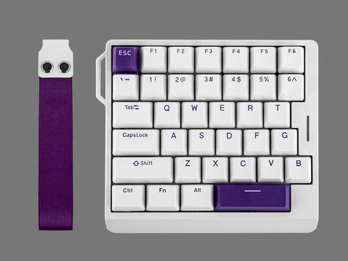
EPOMAKER Unveils HE30: A One-Handed Magnetic Switch Keyboard for Gamers
EPOMAKER introduces the HE30, a compact one-handed magnetic switch keyboard for gamers, boasting an 8kHz polling rate and ultra-precise Rapid Trigger technology for a competitive edge.
-

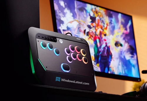
HyperX at CES 2026: Unveiling a TMR Arcade Controller and Magnetic Switch Keyboards
HyperX is set to unveil its CES 2026 lineup, including a groundbreaking TMR arcade controller, advanced magnetic switch keyboards, and a revamped NGENUITY software ecosystem.
-

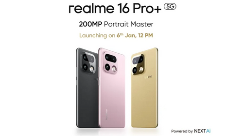
realme 16 Pro+ Specs Revealed: Snapdragon 7 Gen 4, 200MP Camera, and a Massive 7000mAh Battery
realme unveils the 16 Pro+ with a Snapdragon 7 Gen 4 chip, a 200MP camera, and a massive 7000mAh battery, targeting the upper mid-range market.
-

The $30 Kodak Camera That's Selling Out: Nostalgic Genius or a Final Struggle?
Kodak's Charmera keychain camera is a viral sensation despite its poor image quality. This tiny, retro-inspired gadget combines nostalgia with a clever blind-box marketing strategy.
-

Honor WIN Hands-On Review: A 10,000mAh Gaming Beast with a Built-in Fan and 3x Telephoto
The Honor WIN gaming phone pushes boundaries with its massive 10,000mAh battery, active cooling fan, and a versatile 3x telephoto lens, delivering performance beyond expectations.
-

Xiaomi 17 Ultra In-Depth Review: Continuous Optical Zoom + APO Triplet Lens—Has the Phone of the Year Arrived Early?
An in-depth look at the Xiaomi 17 Ultra, featuring a revolutionary continuous optical zoom camera, an APO lens, and exceptional image quality that sets a new industry standard.
-

Honor 500 Pro Review: A Textbook Mid-Range Phone with Exceptional Feel and Battery Life
The Honor 500 Pro raises the bar for mid-range phones with its stunning design, powerful 200MP camera, marathon 8000mAh battery, and flagship-level performance. A true all-rounder.
-

DJI Osmo Action 6 Review: The New Pinnacle of Action Camera Image Quality?
The DJI Osmo Action 6 sets a new standard with its groundbreaking variable aperture, versatile square sensor, and phenomenal battery life, making it the ultimate tool for action videography.
-

Insta360 X4 Air Review: Making 360 Cameras Accessible and Beginner-Friendly
The Insta360 X4 Air balances 8K quality, portability, and an affordable price, making it the perfect beginner-friendly 360 camera for capturing everything.
-

Nothing Ear 3 Review: Where Striking Design Finally Meets Its Sonic Match
The Nothing Ear 3 stands out with its iconic transparent design and finally delivers a balanced, impressive sound quality, making it a rare blend of style and substance.
-

Redmi K90 Pro Max First Look: Is Game-Changing Audio the Key to Success?
The Redmi K90 Pro Max review: A flagship that stands out with its top-tier performance and a revolutionary BOSE-powered 2.1 sound system, carving a new path.
-

iQOO 15 Review: Perfect Gaming Performance, But Photography Has Its Limits
The iQOO 15 delivers flawless gaming performance with its new Snapdragon chip and 2K 144Hz screen, but its camera capabilities reveal some trade-offs for its gaming-centric design.
-

Global OLED Market 2025 Forecast: Samsung Display to Lead with 41% Revenue Share, Says CounterPoint
CounterPoint Research's 2025 OLED market forecast shows Samsung Display leading with 41% revenue share, amidst a market recovery driven by laptops and monitors.
-

The Rise and Swift Fall of the Camera Button: Is Apple's Experiment Over?
Apple's camera button, once hailed as a pro feature and copied by rivals, is rumored to be on its way out. Here’s what went wrong.
-

Report: Nintendo Switch 2 Cartridges to Use 3D NAND for Lower Costs and Higher Capacity
A report from supply chain partner Macronix suggests Nintendo Switch 2 game cartridges will utilize 3D NAND flash, aiming for lower costs and larger storage capacities.
-

Global Smartphone Market Hits Record $100B in Q2 2025, Apple Dominates Revenue
The global smartphone market reached a record $100 billion in revenue in Q2 2025, with Apple capturing 43% of the total, according to a new Counterpoint Research report.


